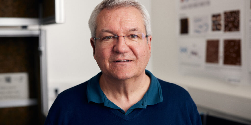
As part of the InCamS@BI transfer project, the Analytics and Materials Development research group is looking for new methods to analyse plastics. Professor Dr Andreas Hütten and PhD student Judith Bünte from Bielefeld University use electron beams to uncover atoms, lattice structures, and layer systems. After all, plastics can only be integrated into a circular economy if we know their precise constituent parts. Researchers from Bielefeld University and Bielefeld University of Applied Sciences are working together for InCamS@BI.
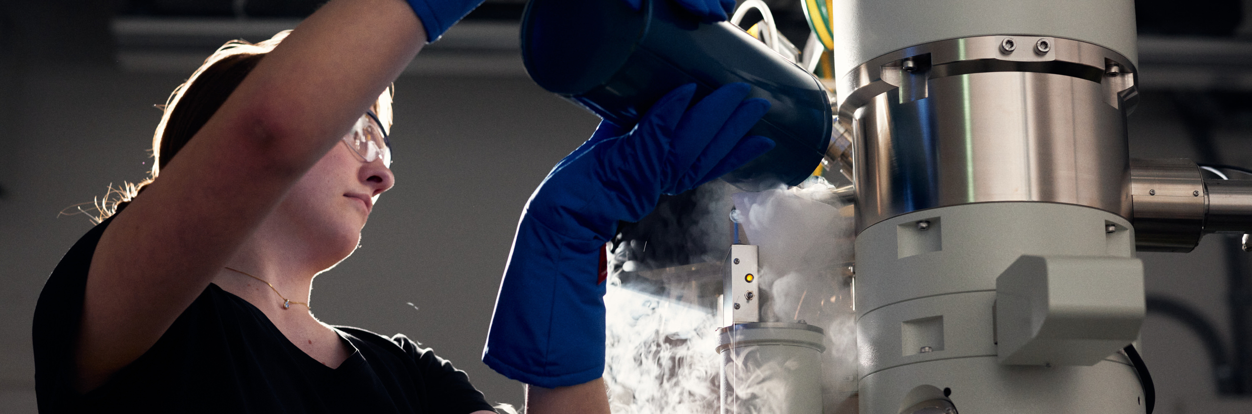
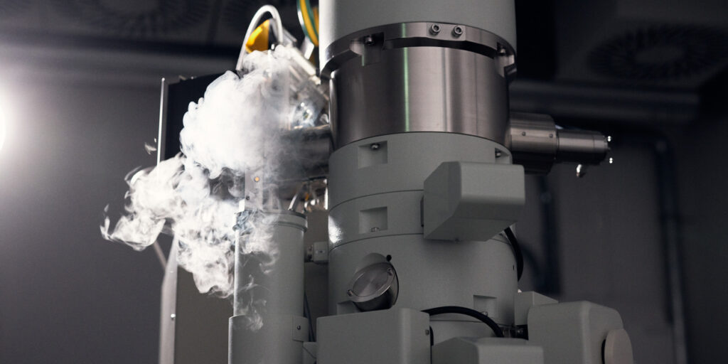
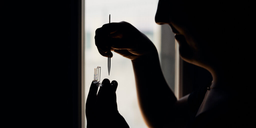
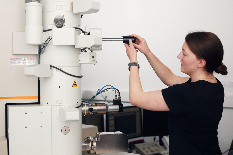
Wearing protective goggles and gloves, Judith Bünte carefully opens an inconspicuous container and removes a cylindrical object. Bünte pours the vapour venting from the top of the cylinder into a three-metre tall device: the transmission electron microscope. This is vapourizing liquid nitrogen, and the experimental physicist uses it to keep her samples clean. Although she is currently still working with metal samples, she would like to analyse plastic samples in the future. She conducts research at InCamS@BI, the Innovation Campus for Sustainable Solutions at Bielefeld University and Bielefeld University of Applied Sciences (HSBI) that is coordinated by HSBI. In the university’s experimental physics laboratories, she demonstrates the equipment she uses for her work.
© Patrick Pollmeier/HSBI
Scanning samples with the electronic beam
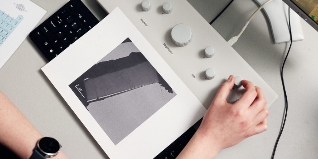
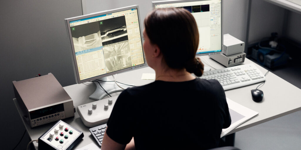
The entrance to the modern building is glazed and the neon yellow walls can be seen clearly through the façade. Visitors pass through three doors and then find themselves in a small corridor which provides access to the clean room, the scanning electron microsopy (SEM), and the transmission electron microscope (TEM). Anyone expecting just a small microscope on a table will be surprised: room E0-311 houses a huge, bulky grey device that takes up most of the space and is connected by cable to various other pieces of equipment. On a desk next to the TEM, there are various control units, three screens, a keyboard, and a mouse. Bünte is well versed with the TEM—she spent a lot of time here while doing her master’s dissertation at the university.
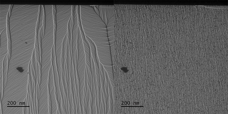
In a TEM, electron beams are directed at a sample and, if it is thin enough, they will penetrate it. The electrons are scattered through the sample and ‘caught’ by a detector on the other side. Depending on which atoms they encounter, they will behave differently. For example, the different interactions impact on the energy and the exit angle. These interactions reveal the areas of the sample from which the electrons are scattered.
© Patrick Pollmeier/HSBI
© Patrick Pollmeier/HSBI
© Patrick Pollmeier/HSBI
© Patrick Pollmeier/HSBI
© Patrick Pollmeier/HSBI
© Patrick Pollmeier/HSBI
© Judith Bünte/Universität Bielefeld
Analysis in a vacuum to avoid interference from air molecules
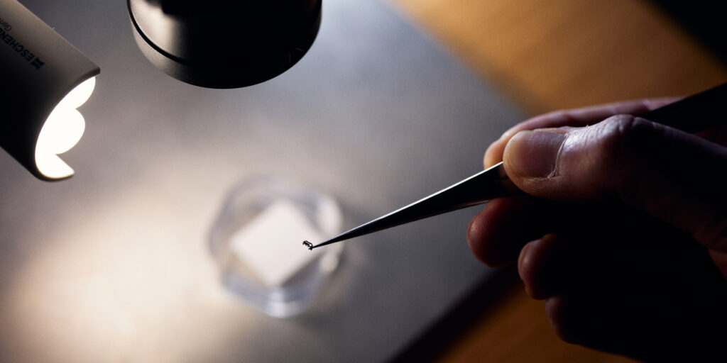
The researcher places the metal sample, which is around three millimetres in diameter, in a holder. ‘This one is a sample of the metal cobalt. A colleague made it in what is known as a sputtering system because we need very thin samples for the TEM. On top of the 50-nanometre-thin cobalt layer, there is a two-nanometre layer of ruthenium to protect the sample from oxidation.’ Bünte pushes the holder into the TEM and flips a switch. The sample is now in an airlock to prevent air from outside entering the device. She fills a Dewar flask on the column of the TEM with liquid nitrogen so that residual gas molecules do not adhere to the sample during the analysis. The liquid nitrogen serves as a refrigerant, because it can maintain a temperature far below the freezing point of water—in this case minus 196.15 degrees Celsius. It cools a copper cooling finger located above the sample in the TEM on which unwanted atoms and molecules condense. This keeps the sample pure and allows analysis in the TEM. There is a vacuum in the device so that air molecules do not deflect the electron beams.
Making atoms in plastics visible
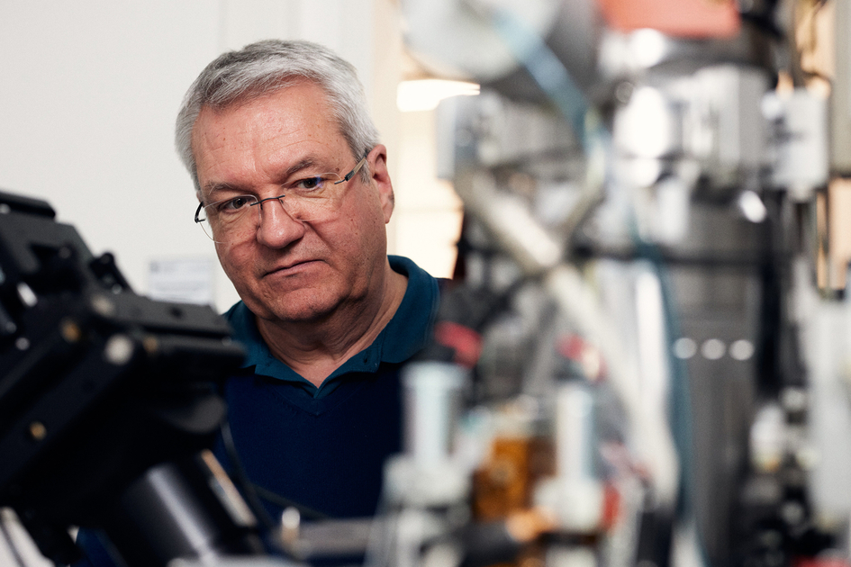
‘We see only tiny sections of the sample here. And they are so minute that we can examine individual atomic columns and crystal lattices,’ explains Bünte, who views the results on the screen together with Professor Dr Andreas Hütten. He is her supervisor, oversaw her first scientific work, and now provides support as her mentor in InCamS@BI. Both belong to the InCamS@BI research group Analytics and Materials Development. The group is based at Bielefeld University and consists of three working groups headed by Professor Dr Andreas Hütten, Professor Dr Harald Gröger, and Professor Dr Dario Anselmetti respectively. Judith Bünte is a technology scout in Andreas Hütten’s group and is doing her PhD with the expert in the physics of nanostructures. He has been researching and teaching at the university since 1997.
© Patrick Pollmeier/HSBI
Back to the laboratory: another device used here is the FIB, which stands for focused ion beam. This cuts a piece out of a sample by means of high-energy ions that is then analysed using the scanning electron microscope (SEM) integrated in the FIB. In contrast to the TEM, the SEM guides an electron beam over the sample in a defined pattern. This beam does not pass through the sample, but is scattered back. SEM, TEM, and FIB are all currently used for metal or organic samples. ‘What I find most thrilling is that I can actually see the atomic column with the microscopes,’ says the PhD student.
The next step: transferring methods for analysing metals to plastics
Bünte’s task in the InCamS@BI project is to test these methods on plastics. ‘We would have to adapt the method depending on the type of plastic,’ says Bünte. ‘The difficulty is that unlike metals, the atoms in plastic molecules are very light. This means that the electrons are barely deflected, and there is not enough contrast in the images. One question researchers are asking is therefore: how can we make plastics more visible?’ Another challenge: plastics are quickly destroyed by the energy of the electron beam. Bünte and Hütten regularly exchange ideas, hold discussions, and try out new things.
Hütten knows that interdisciplinarity pays off: ‘Our team is now building on the analytical work at the Centre for Interdisciplinary Materials Research and Technology Development, or CiMT for short. We have developed toolboxes there to determine the ageing mechanisms of various polypropylene materials, which we can now apply to the challenges of the InCamS@BI project.’ The Analytics and Material Development research group is now working on a toolbox for optimizing the reuse of plastics. Such toolboxes should help companies achieve circular economy in the future.
© Patrick Pollmeier/HSBI
Contributing to sustainability
‘The deeper I get into the topic of plastics on a scientific level, the more difficult it seems to me to communicate this topic to society, to non-specialists, to laypeople not familiar with the natural sciences,’ says Bünte. This is also one of the aim’s of InCamS@BI: to exchange knowledge and ideas not only with industry but also with society. And materials research in the field of plastics is particularly relevant for them: hardly anyone can get by without plastic products in everyday life. ‘There are lots of challenges associated with plastics—the littering of our oceans is just one of them. I find it all the more exciting that here in Bielefeld, in research, we can make a contribution to greater sustainability.’
InCamS@BI
Sustainable materials research is the focus of InCamS@BI, the Innovation Campus for Sustainable Solutions. The joint project generates ideas and develops solutions to optimize plastics and their utilization for a circular value creation (circular economy): which plastics are suitable for reuse, and what is the best possible way to process them? How can products be adapted to use recycled plastics? How can consumers be better involved in the journey to circular use? To find answers to these questions, Bielefeld University and Bielefeld University of Applied Sciences organize the exchange between academia, industry, and society in InCamS@BI with innovative formats and an interdisciplinary team. InCamS@BI is funded by ‘Innovative University’, an initiative of the German federal and state governments, totalling 8.8 million euros from 2023 to 2027.